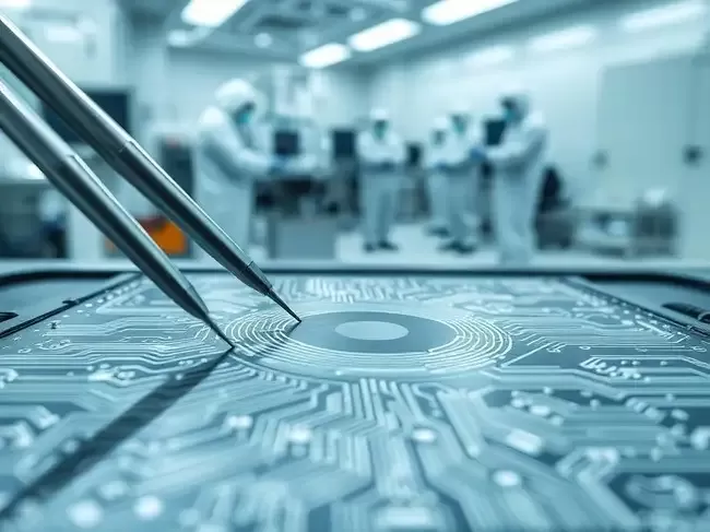
India is positioning itself to take a leap in semiconductor technology by focusing on the development of 2D materials, which could potentially create chips far smaller than current silicon-based counterparts. A proposal led by the Indian Institute of Science (IISc) seeks government approval for a Rs 500 crore investment to develop these materials and establish India's foothold in next-generation chip manufacturing. This initiative could place India in direct competition with leading global players in semiconductor technology, such as the US, Japan, and South Korea, by developing angstrom-scale chips. However, the clock is ticking, and India must act swiftly to capitalize on this opportunity.
India’s Ambitious Semiconductor Leap: The 2D Materials Proposal
In an effort to push the boundaries of semiconductor technology, India is exploring a revolutionary project to develop 2D materials capable of manufacturing chips at an angstrom scale — a technological leap from the current nanometer-scale chips dominating the market. At the forefront of this initiative is a detailed project proposal submitted by a team of scientists from the Indian Institute of Science (IISc). This report, initially submitted in April 2022 and revised in October 2024, envisions a transformative shift in India’s semiconductor manufacturing capabilities, positioning the nation to compete globally in this critical technology.
The project hinges on the development of ultra-thin materials such as graphene and transition metal dichalcogenides (TMDs). These materials, expected to replace traditional silicon in semiconductor fabrication, offer the potential to produce much smaller and more efficient chips. While the global semiconductor industry is currently dominated by the production of 3-nanometer chips, 2D materials promise to create chips far smaller, operating at the angstrom scale. This advancement would mark a significant technological leap, propelling India into the global semiconductor race.
Government Support and Global Investment Landscape
India’s push to develop cutting-edge semiconductor technologies comes at a time when the global market for such materials is experiencing a surge of interest. Countries like the US, Japan, and South Korea have already invested significantly in 2D material research, with Europe investing over USD 1 billion (around Rs 8,300 crore) into the development of these materials. Other nations, including China and Japan, are also allocating undisclosed funds to advance their semiconductor capabilities.
The Indian government, through the Ministry of Electronics and Information Technology (MeitY), has shown support for the project, acknowledging its potential. Discussions are underway to explore where 2D material-based semiconductors could be deployed within India's electronics ecosystem. The Principal Scientific Adviser (PSA) office, in collaboration with MeitY, the Department of Space, and other key stakeholders, has been actively engaging with the IISc-led team to assess the project’s feasibility and strategic importance for India’s technological future.
In comparison to other global initiatives, the IISc-led proposal seeks a modest Rs 500 crore over five years. This funding is intended to develop indigenous technologies capable of fabricating angstrom-scale chips. The proposal also includes a roadmap for self-sustainability post-funding, ensuring that the project can continue to thrive independently in the long term.
The Strategic Importance of Semiconductor Independence
Semiconductors are at the heart of the global tech industry, powering everything from smartphones and computers to automobiles and defense systems. In India, the reliance on foreign semiconductor suppliers has been a growing concern, particularly given the strategic importance of these materials in both economic and national security contexts. Currently, India depends heavily on global players for semiconductor manufacturing, but the shift toward 2D materials could reduce this dependency and position India as a leader in the next generation of semiconductor technologies.
The nation's largest semiconductor project, a collaboration between Tata Electronics and Taiwan's PSMC, is already underway with an investment of Rs 91,000 crore under the India Semiconductor Mission. This project, eligible for 50% capital support from the government, aims to establish a substantial manufacturing base for semiconductors in India. However, the IISc-led initiative provides a different approach, focusing on the development of next-generation, ultra-small chips that could push the limits of current technology.
Urgency and Global Competition
Despite the promising nature of the IISc proposal, some experts within the research community have raised concerns over the pace of India’s progress in the 2D materials space. According to an officer familiar with the global research landscape, time is of the essence. "Global momentum is building around 2D semiconductors, and India’s efforts, while promising, are still limited and need urgent scaling," said the officer. The ongoing deliberations and lack of formal assurances from the government could potentially derail India’s chance to take a leadership role in the field.
While countries around the world are already preparing for a post-silicon future, India is still in the stage of discussions and planning. The global demand for advanced semiconductor technologies is accelerating, and India's window to act may soon close. The IISc proposal, which requests relatively modest funding compared to other global semiconductor projects, represents a critical opportunity that could provide India with a competitive edge in this key sector.
Conclusion: A Pivotal Moment for India’s Semiconductor Future
As the world’s semiconductor industry advances toward smaller and more powerful chips, India stands at a crossroads. The IISc’s 2D materials project represents a crucial opportunity for the country to break free from its dependence on foreign semiconductor technologies and establish itself as a global leader in cutting-edge electronics. However, to succeed, India must move swiftly from deliberation to action, securing the necessary funding and resources to support the development of these next-generation materials. With global players already pouring significant investments into 2D materials research, India’s timely response to this emerging field will determine its ability to lead in the semiconductor industry for years to come.
Comments